What is PCB and How to design explaining step by step?
Printed Circuit Boards (PCBs) have become an essential part of modern electronic devices. They are used to connect electronic components and provide a platform for signals to flow between the components. Whether you’re a hobbyist or a professional, knowing how to design your own PCBs is an important skill to have. In this article, we will explore what PCBs are and provide a step-by-step guide on how to design your own.
What is PCB?
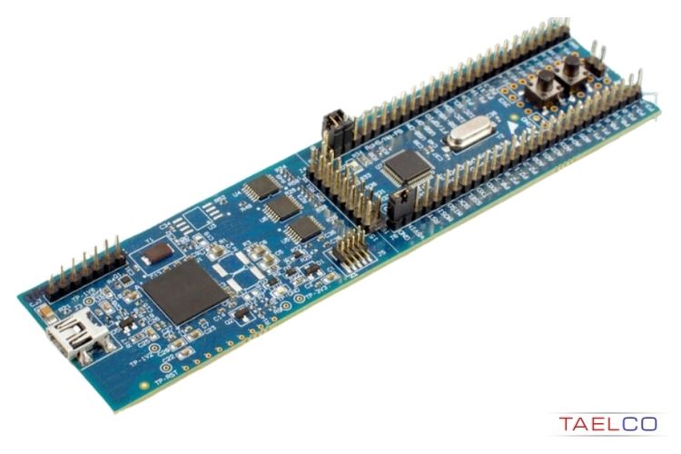
A PCB is a board made out of a non-conductive material, with thin copper conductive tracks laid out on its surface. These tracks connect various electronic components of an electronic circuit, providing support and structure to the circuit. PCBs are typically designed with the help of a computer-aided design (CAD) software.
Step-by-step guide on designing PCBs:
Schematic design:
Before starting the PCB design process, it is important to have a schematic of the circuit you want to design. A schematic shows how the electronic components of the circuit are connected to each other. There are many schematic capture software options available in the market, such as Eagle, KiCad, or Altium Designer.
PCB Layout design
Once you have the schematic design, it is time to create the physical placement of the components on the board. This is done using a PCB layout tool. The tool allows you to place the components on the board in a way that facilitates their connection through the copper traces. Rearranging the components and tracks during the design process can be done as required until an optimal solution is obtained.
Routing
Routing is the process of designing the tracks using the layout design. The copper tracks are used to connect the components to each other in the schematic diagram. During routing, you will have to ensure that your tracks are wide enough to carry sufficient current and also that tracks are not too close together to avoid a short circuit. The PCB layout tool will usually have auto-routing functionality, but it is often better to take manual control of routing to ensure a better routing layout.
Fabrication
After the PCB design becomes complete, this is the time to get it fabricated. PCB fabrication is the process of creating the physical board. There are many PCB manufacturing vendors available that can produce high-quality boards and can also give you specifications for PCB fabrication processes that they can perform.
Assembly
Once the board is fabricated, it is time to assemble the electronic components on the board. This can be done either by a professional circuit assembly shop or by yourself if you have the necessary equipment and tools. The assembly process involves placing the electronic components and soldering them onto the board.
In summary, designing a PCB can be an enjoyable task for electronics enthusiasts. But for newcomers, it can seem like a daunting task to start with. Fortunately, CAD software and PCB manufacturing firms have made the task simpler by providing users with various easy-to-use tools and templates, letting anyone learn the PCB design process. By following the steps outlined in this article, you can design your own PCBs and bring your electronic projects to life with ease.
In this article, we have explained in detail “What is PCB and How to design explaining step by step?” which is a frequently asked question in the aviation industry. If you are interested in aviation and engineering fields, you can read NASA as a global source and other articles on the TAELCO Blog as a Turkish source.


Leave A Comment